
21 September 2026, NIICE Commentary 12751
Himadri Agarwal
Today, nearly 20 percent of the world’s semiconductor design engineers are in India yet we import almost 95 percent of chips from China, Taiwan, South Korea, and Singapore. This paradox lies at the heart of its semiconductor ambition. While recent investments and projects signal progress, the real question remains—are we building technological capability or merely assembling participation? This article examines India’s semiconductor policy journey through the lens of the Tata Electronics case study, offering a critical assessment of what has been achieved and what remains aspirational.
The Semiconductor Paradox
India represents a missed opportunity in the semiconductor industry; we were well positioned in the race, even ahead of giants like Taiwan in the 20th century yet lost that power due to a massive setback in 1989 when a devastating and mysterious fire gutted the entire Semiconductor Laboratory (SCL) facility. In the decades that followed, the “License Raj” and slow decision-making discouraged foreign investments from major Silicon Valley firms, which then reallocated to Malaysia and Vietnam owing to India’s restrictive policies.
Chips as the New Oil: Strategic Importance
The urgency of these failures lies in the immense value of semiconductors who have emerged as the “new oil” in geopolitics. While oil powered the industrial age, these chips have been the invisible engine of the digital era-essential in almost every piece of equipment, ranging from smartphones to electric vehicles to advanced medical devices. Modern warfare relies on these chips for precision-guided missiles, stealth technology, and encrypted communications. This strategic importance is evident in how nations like the United States and China are investing billions to secure supply chains, while Taiwan’s dominance through TSMC has made it central to global technological stability. Hence, it will not be an assumption to make that the nation that controls its supply will hold immense diplomatic power in global politics.
Policy Push: Building the Foundation
In recent years, India has been trying to transition itself from passive importer to an active architect of its semiconductor future through a series of policy shifts. To lay down the foundation, in 2020 schemes like the Scheme for Promotion of Manufacturing of Electronic Components and Semiconductors (SPECS) and the Production Linked Incentive (PLI) were launched to provide 4-6 percent incentives on incremental sales to boost domestic component manufacturing. In 2021, under India Semiconductor
Mission 1.0 (ISM), the government announced an INR 76,000 crore outlay providing 50 percent fiscal support for semiconductor labs and display fabs alongside a chip design support fund. To train engineers, in 2022 the government started a Chips to Startup (C2S) programme accompanied by MoUs with the USA, Japan, the EU and Singapore. From all of the efforts, it can be inferred that the pillars of the foundation of manufacturing were taking shape. Subsequently, the government has approved ten major units, including Tata-PSMC Fab in Dholera, Micron Technology (ATMP) and Kaynes Semicon OSAT in Sanand, Gujarat. Among these, the Tata- PSMC Fab stands as the single most consequential project in India’s semiconductor journey.
Tata Electronics: A Case Study in Ambition
Tata Electronics has been allocated a total investment of over ₹1.18 lakh crore, distributed across two distinct projects- the Mega Fab in Dholera, Gujarat, and Tata Semiconductor Assembly and Test Pvt. Ltd. (TSAT) facility in Jagiroad, Assam. Together, these units are designed to cover the entire lifecycle of a chip—from manufacturing raw silicon wafers in Gujarat to final packaging and testing in Assam.
The Mega Fab is a high-technology “foundry” allocated ₹91,000 crore (~USD11 billion) in partnership with Taiwan’s PSMC firm. Its major objectives include producing 50,000 wafers per month, focusing on 28nm, 40nm, 55nm, 90nm, and 110nm nodes for applications in AI, electric vehicles (EVs), telecom, and high-performance computing. Civil Construction is progressing on schedule, with the first chip production targeted for late 2026. Tata Semiconductor Assembly and Test Pvt. Ltd. (TSAT) facility in Jagiroad, Assam, allocated ₹27,000 crore, can process 48 million chips per day using Flip-Chip and ISIP technologies, and is expected to be commissioned by April 2026.
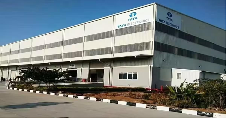
Figure1: Tata Electronics, The Mega Fab Plant in Dholera, Gujarat
Analysis and Arguments: Progress Without Power?
Manufacturing a semiconductor chip is akin to constructing a multi-story skyscraper, but the entire building is smaller than a grain of rice. The process begins with purifying silica into silicon, growing it into ingots, and slicing these into circular wafers. In this inception itself, India imports 80-90 percent of its wafers and lacks the domestic infrastructure for high- purity silicon production.
In the fabrication phase, processes such as photolithography, etching, Ion implantation (Doping), and deposition create the chip’s intricate architecture. India’s current focus on 28nm nodes is adequate for automotive and consumer electronics but falls significantly short of the 3nm or 2nm chips powering the latest smartphones and AI servers. This technology gap is not trivial-it signals that India is entering the semiconductor race, but not at its technological frontier. The chips required for cutting- edge applications will continue to depend on imports for the foreseeable future.
Infrastructure reliability presents another formidable challenge. Semiconductor fabs demand 100 percent uninterrupted, high-quality power and water supply; even a one-second power flicker can ruin an entire batch of wafers worth millions of dollars. Tata’s response includes constructing an “elephant- proof wall” and employing a full-time snake rescue team at Jagiroad, Assam, to prevent wildlife-induced vibrations from disrupting precision manufacturing. While innovative, the true reliability of this infrastructure can only be validated once production commences-India is still perfecting the stability standards that established fabs take for granted.
The workforce gap is perhaps the most critical structural constraint. India possesses thousands of world-class chip designers but critically lacks fab operators-professionals trained to run multi-billion- dollar cleanroom machines without compromising wafers that cost anywhere from USD 5,000 at 28nm to over USD 20,000 at advanced 3nm nodes, the very frontier India aspires to reach by 2032. To address this, Tata is sending engineers in batches of 50-75 to Taiwan’s PSMC for training programmes in yield engineering and process technology. However, industry experts raise valid concerns about retention: will these engineers return to India, or will they be drawn to higher salaries in Taiwan or the United States? Even with full retention, the Dholera plant alone will require at least 20,000 skilled workers-a figure that makes the current training programme a preliminary step, not a solution.
Conclusion: A Beginning, Not a Breakthrough
The case of the Tata Dholera facility reveals that India’s semiconductor mission is far more complex than public discourse often suggests. What is frequently presented as a breakthrough is, upon closer examination, only the beginning of a long and demanding process. India’s recent policy push marks a significant shift in intent and direction. Yet the country remains structurally constrained by gaps in technological depth, workforce readiness, and infrastructure reliability. The transition from policy ambition to industrial capability will require years of sustained effort across multiple fronts simultaneously. Projects like Tata’s Dholera facility signal direction, but not yet dominance. Without moving beyond assembly into genuine innovation, India risks remaining a participant in the semiconductor race rather than emerging as a leader. The challenge before India is not merely to manufacture chips, but to build the capacity, capability, and continuity required to shape the future of the global semiconductor order.
Himadri Agarwal is currently pursuing her B.A. program at Kanoria PG Mahila Mahavidyalaya, RU, India.